HP 4951B Protocol Analyzer

Got it for next to nothing on ebay, but it lacked its pod cable.

Documents and links:

From the HP Computer Museum website:

  • The 4951A operation manual

04951-90003_4951A_OperatingManual_129pages_Apr84.pdf

  • The 4951C operation manual

04951-90702_4951C_OperatingManual_312pages_Aug86.pdf

  • The 4951A Service Manual

04951-90002_4951A_ServiceManual_209pages_Apr84.pdf

  • The 4951C Service Manual

04951-90703_4951C_ServiceManual_393pages_Nov86.pdf

Cable pinout

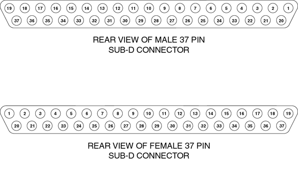
From the 4951C service manual (page 210), these are J2’s pin assignments on the device:
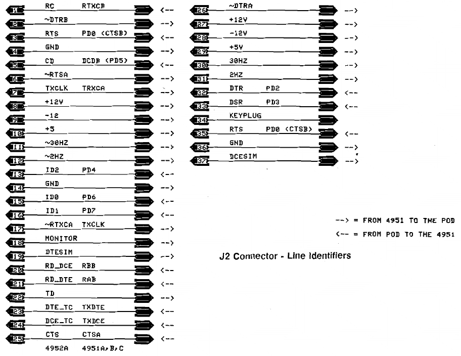
The J2 line identifiers from the service manual, with the direction of each signal: pin 26 carries ~DTRA from the 4951 to the pod.
The 37-pin sub-D numbering seen from the rear, male above and female below, for working out which physical pin is which.

The schematic for the CPU and DLC part of the analyzer is this (figure 8-14):
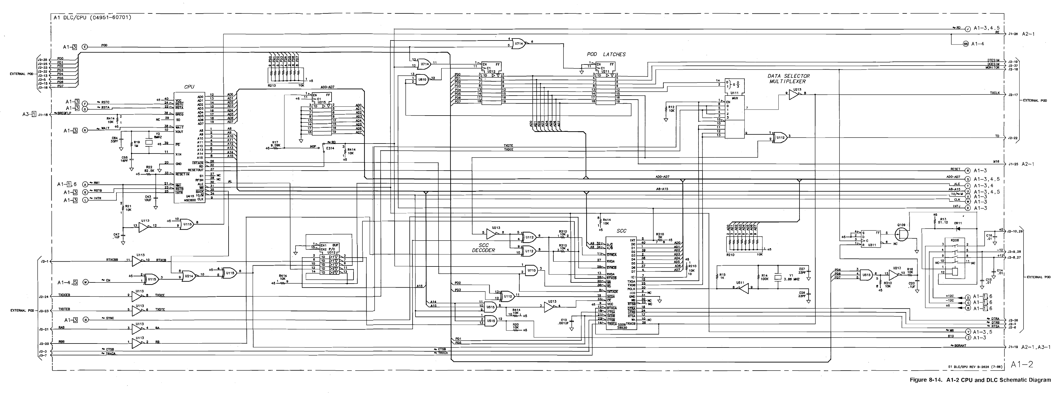
Figure 8-14, the A1-2 CPU and DLC board. The Z8530 SCC is in the lower middle, with the pod latches and the data selector multiplexer feeding J2 along the top.

The information on the 18179A RS232 POD starts around page 350 in the service manual. The interface connector there is called J1 and it has the following assignments visible:
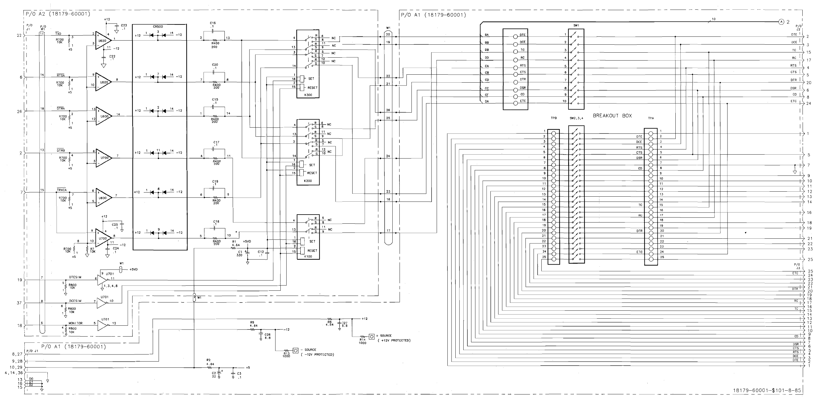
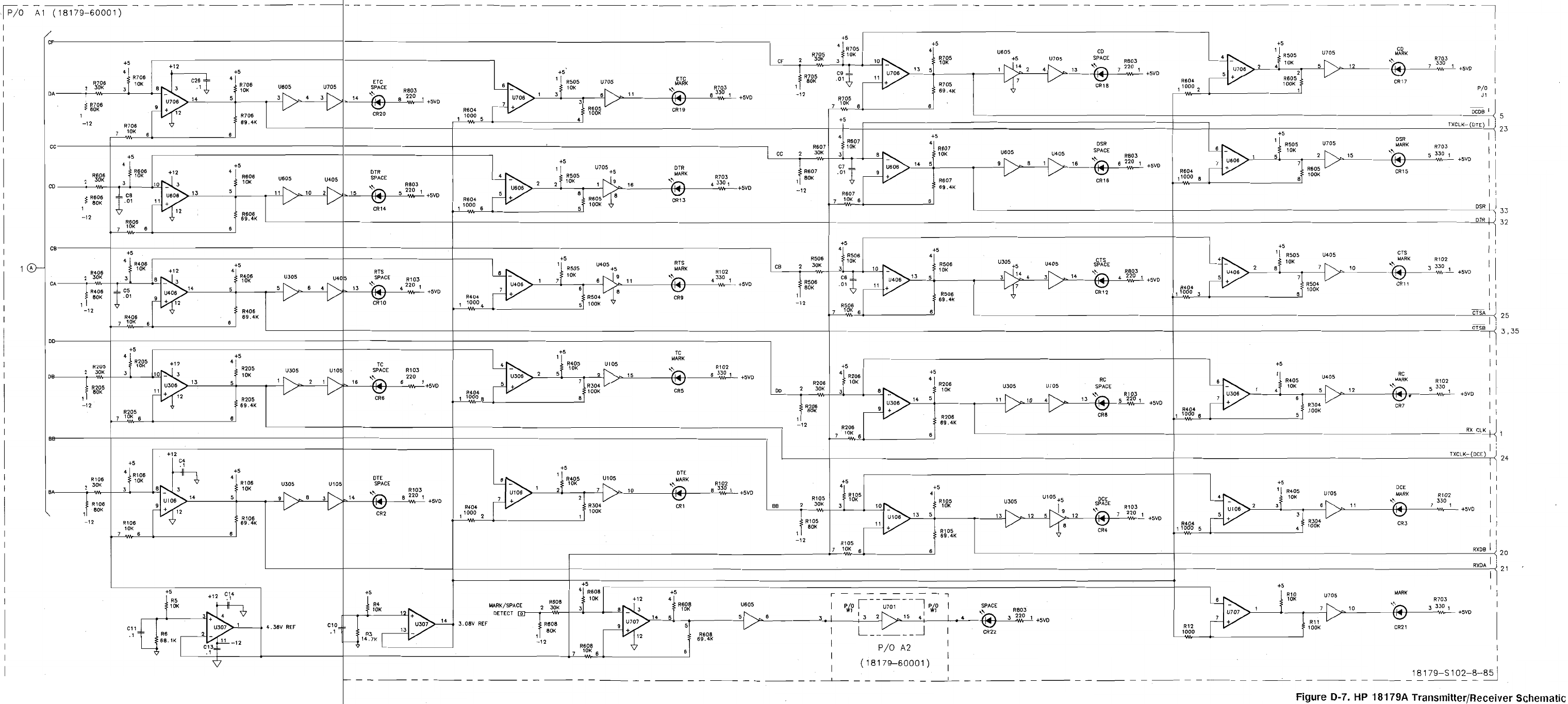
The 18179A pod, sheet 1: the line receivers at the left, the K100 to K300 latching relays in the middle, and the breakout box switch matrix on the right.
Sheet 2, the transmitter and receiver section. Each control line gets its own mark and space comparator pair driving an indicator LED.

This seems to be a straight-through cable. Sadly enough the EXT test still fails with such a cable installed 8-/

The SCC seems the most likely problem. This is a Zilog Z8530CS according to the schematic diagram (page 217), A1U209.

Pictures
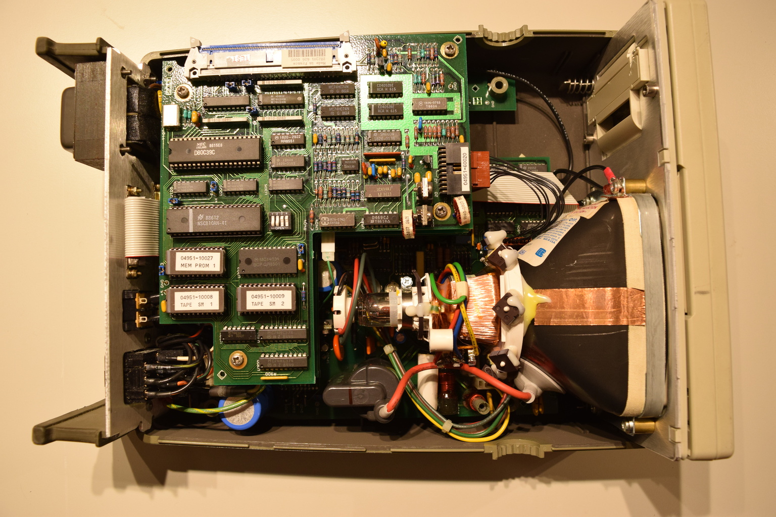
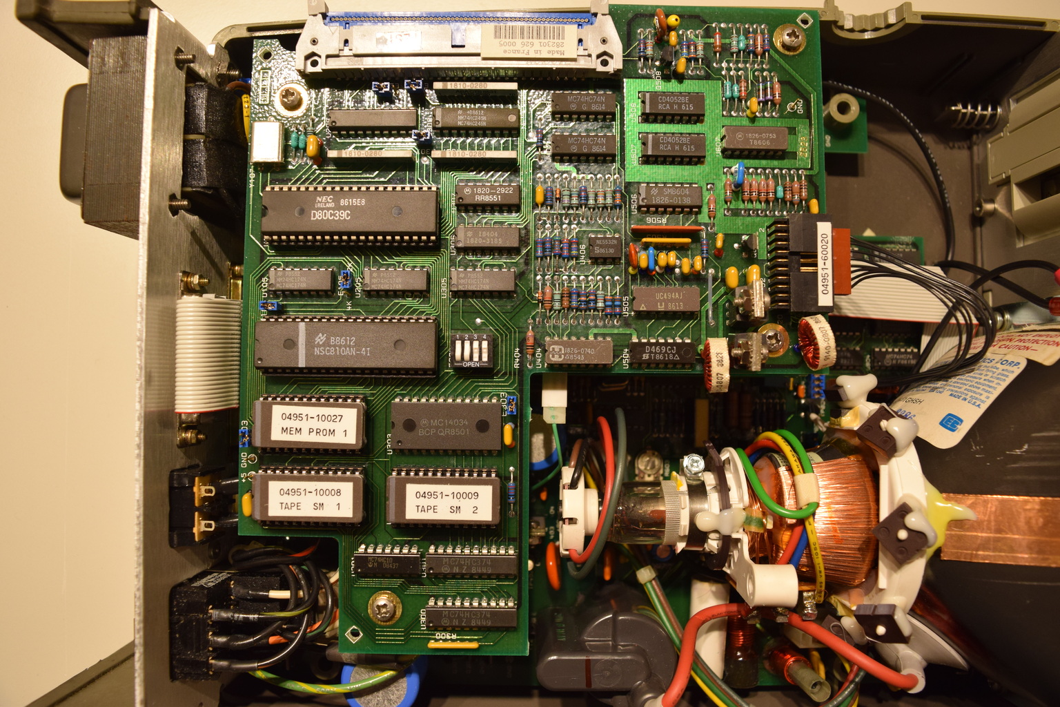
The analyzer opened up, with the CRT at the right and the CPU board carrying MEM PROM 1 and the two TAPE SM PROMs at the left.
The same board closer in: the NEC D80C39C at the top left, the NSC810AN-4I RAM/IO below it, and the 04951-10008/10009 tape state machine PROMs at the bottom.
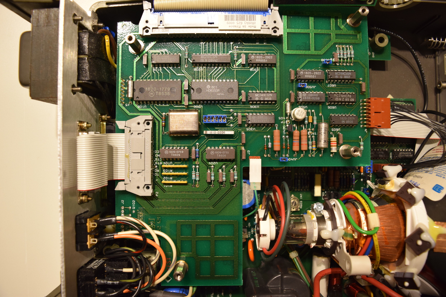
A second board with an HD6350P and a 1820-1779 in the middle, and the ribbon to the front panel connector at the left.
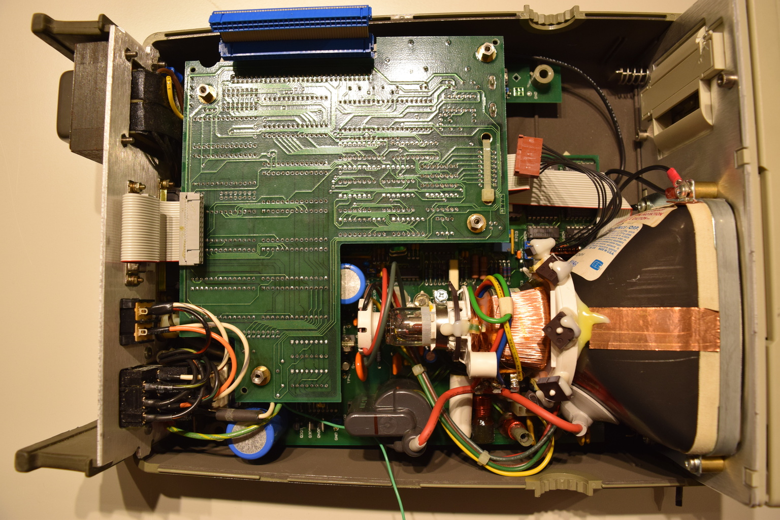
The solder side of the top board, showing how little is actually on it.
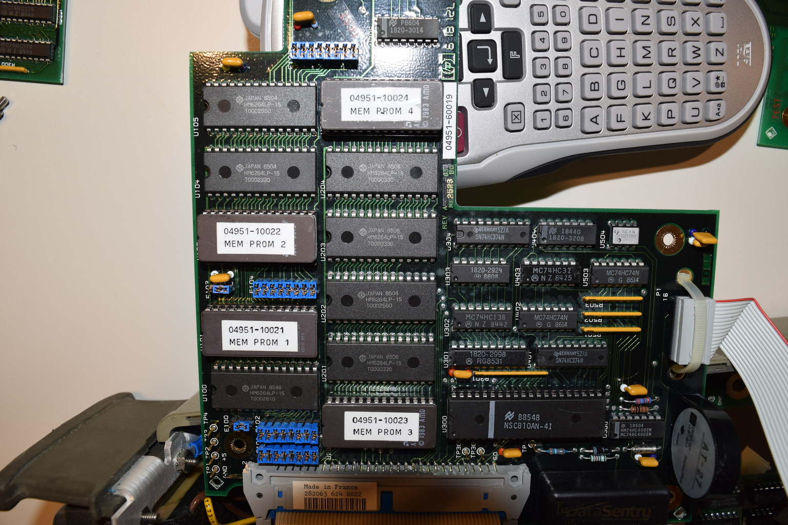
The memory board lifted out: four MEM PROMs and six HM6264LP static RAMs, with the keypad resting alongside.
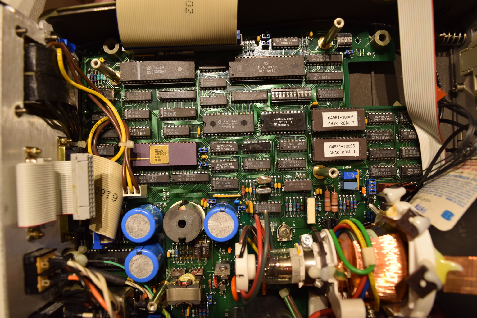
The board carrying the fault. The purple ceramic Zilog Z8530CS SCC sits at the left of centre, next to the MC68A45P CRT controller and the two CHAR ROMs.

Fixing the issue

The machine seems to work fine, but the pod selftest fails.

I entered a simulate program to test the pod (the DTE test as described in the service manual for the 18179 pod around page 350). This sends data and toggles the rts and dtr lines. Running this program shows dtr nicely flashing on and off- but dtr remains space.

Following the schematic diagram for the CPU card we see that _DTRA_ (negated) leaves from pin 16 of the scc. The oscilloscope confirms that there is an inverse signal there.

Probing the same signal on the pod print (the small print containing the input opamps) on U600 pin 13 shows no pulse. Conclusion: the cable is bad. Checking continuity on the cable indeed showed a single pin not being connected (pin 26)..

Re-pressing the cable solved the issue, and the test now passes.

Time to put the whole thing together again…

Last modified: 2026/09/06